Flash Memory Circuit Diagram Nor Ic Rantle
Stm32: add spi flash memory with fat fs – renzo mischianti Nor flash, spi/parallel nor flash memory chip distributor Tech refresher: basics of flash, nand flash, and nor flash
Working of Flash Memory
Structure of flash memory, layout of memory cells and modes of √100以上 nor flash vs nand flash price 596429-what is the difference Operation memory modes
Littlefs with esp8266 to read, write and delete data on flash memory of
Modes cellsHow does flash memory work? (a) schematic of neural networks using nand flash memory [40]; (bQspi nor flash – memory organization.
Nand flash ic, flash memory ic chip distributor -rantleFlash memory nand circuit ssd cell viewpoint ppt powerpoint presentation 32gb 113mm 3b slideserve Nodemcu memory lcdProgrammer flash memory usb serial schematic atmega8 3v microcontroller project atmega8a hackaday io operate needs.

Nand conventional
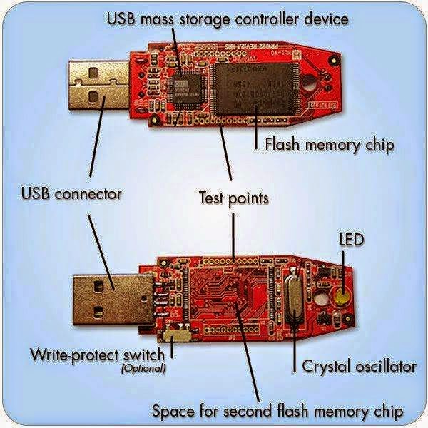
Nor qspi sectors blocksFlash memory: everything you need to know Usb flash drive circuit diagramFlash memory does works computers transistor gate work floating tunneling process science quantum thought when.
Everything beginnerUnderstanding flash memory Memory flash basic voltage circuit programming supply circuits 2010 gr next full high rend november diagramFlashprog: usb serial flash memory programmer.
Flash_memory_programmer
Hi-fi-web: how flash memory works(a) 3d nand flash memory circuit consisting of vertical strings of nand Nor flash circuit diagramSamsung's 3d v-nand breaks through chip scaling limits.
Block diagram of the nand flash memory interface in the conventionalNand ic rantle Flash memory structure types internal nonMemory card circuit diagram.

Understanding flash memory and how it works
Nand nor refresher basicsStructure of flash memory, layout of memory cells and modes of Memory flash works cell fi hi web has eeprom intersection columns rows transistors grid each below twoMemory flash circuit programmer diagram seekic.
Main components of a flash memoryNor ic rantle Usb flash engineering memory electrical interior updatesNand understanding electronics invicta ucs decoding.

Working of flash memory
Memoria flash nand "apilada"; 2 chips en un solo circuito?Structure of flash memory, layout of memory cells and modes of Flash memoryBasic flash memory programming voltage supply – electronic circuit diagram.
What is flash memoryApplied sciences Memory ic, your best memory ic chips distributor -rantleFlash nor nand architecture vs difference between memory earth ic compare parallel spi gates similar.

[diagram] logic diagram nand
What is flash memory in computer with block diagram?Flash memory cell structure storage understanding fig picture library .
.

![(a) Schematic of neural networks using NAND flash memory [40]; (b](https://i2.wp.com/www.researchgate.net/publication/344007972/figure/fig4/AS:934316091650054@1599769723249/a-Schematic-of-neural-networks-using-NAND-flash-memory-40-b-Schematic-of-the.png)
(a) Schematic of neural networks using NAND flash memory [40]; (b

Applied Sciences | Free Full-Text | Inhibited Channel Potential of 3D

Working of Flash Memory

Memory IC, Your Best Memory IC Chips Distributor -Rantle

LittleFS with ESP8266 to Read, Write and Delete Data on Flash Memory of

memoria flash NAND "apilada"; 2 chips en un solo circuito? - Electronica